
In this chapter, you learn how to test your CMOS inverter with Spectre in Cadence Analog Design Environment (ADE). You will see the switching action of the inverter, measure how long the output takes to respond (propagation delay), and find how the output voltage changes as you sweep the input voltage (Voltage Transfer Curve, or VTC).
First complete the inverter schematic and symbol. Your inverter should have four pins: vin, vout, vdd, and gnd.
You will work through four stages: build a testbench, save a simulation setup, run and measure a transient response, and sweep the input voltage. An additional transistor strength simulation shows how to run a parametric simulation.
The names of the different tools and windows may be confusing at first. ADE Assembler is used to organize your simulation tests, while ADE Explorer is used to configure and run an individual test. Spectre is a circuit simulator that performs the actual simulation, and the Virtuoso Visualization and Analysis (ViVA) tool is used to display and analyze the resulting waveforms.
1. Build a testbench
Your inverter schematic describes the circuit you created. To simulate it, you need a separate test circuit that provides power, drives the input, and applies a load to the output. We often call this type of test circuit a testbench. Keeping the testbench in a separate cell allows designers to reuse transistor-level circuits (such as the inverter you just created) in other designs.
In the Library Manager, choose File → New → Cellview. Use yourUNI for the library name, inverter_test for the cell name, and schematic for both the view and type. Click OK.
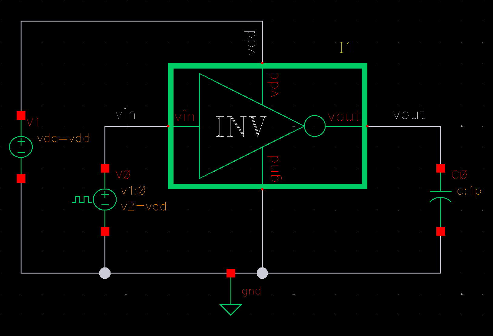
vin. The capacitor loads vout. Both sources and the capacitor share the inverter's ground connection.Place the inverter, sources, capacitor, and ground
Choose Create → Instance to place each component. Alternatively, hit i. Use the symbol view for every component. To edit a component's parameter, select the component and press q.
Enter each number immediately followed by its scale suffix: 1p, 10n, or 1u. Do not insert a space or append the unit. The unit indicator will be populated automatically.
-
Place the inverter. Select
yourUNIlibrary, choose theinvertercell, and place the symbol you created in the schematic tutorial. -
Place the supply source. Select the
analogLiblibrary and thevdccell. Set DC voltage tovdd, then place the source.The name
vddin a source's value field is a design variable. You can specify the value of the variable later in ADE Explorer. Using the same variable for the supply and the pulse's high level sets both voltages equal.
Set the supply source's DC voltage to vdd. -
Place the input source. Select the
analogLiblibrary and thevpulsecell. You will use this periodic square-wave source to drive the inverter input. Enter the following parameters, then place the source:vpulsefieldValue to enter Voltage 1 0Voltage 2 vddPeriod 1u
Select analogLib / vpulse / symboland enter the input source's voltage levels and period.These settings produce a 1 MHz input with a 50% duty cycle.
-
Place the output capacitor. Select the
analogLiblibrary and thecapcell. A capacitor will simulate the effect of capacitive loading from the following stages. For illustration purposes, set Capacitance to1p(1 pF), then place the capacitor near the inverter output. -
Place the ground reference. Select the
analogLiblibrary and thegndcell. Place the ground symbol near the source negative terminals. You will connect the ground symbol to the common ground wire when wiring the test circuit.
Connect every terminal to its intended net
Use Create → Wire (narrow) to make the connections in Figure 1.
Choose Create → Wire Name (alternatively, press l as in 'label') and label the input wire vin and the output wire vout. Press Esc after placing the labels.

vin in the Names field and place the label on the input wire. Repeat with vout for the output wire.
Make sure to connect the ground symbol to the ground net. A pin named gnd alone does not tell the simulator which node should be used as the reference node. The ground symbol explicitly defines the reference node.
Choose File → Check and Save. If there are any connection errors or warnings, fix them before opening ADE.
2. Save your simulation setup in a maestro view
Open inverter_test / schematic if it is not already open. Then, choose Launch → ADE Assembler from the upper-left corner. Select Create New View, verify that the correct library and inverter_test cell are selected, and keep maestro as the view name. Then click OK.
ADE Assembler will open. In the Data View window, locate the Tests section. Click the + icon to expand the menu, then click Click to add test. Select your library, inverter_test cell, and schematic view, then click OK.
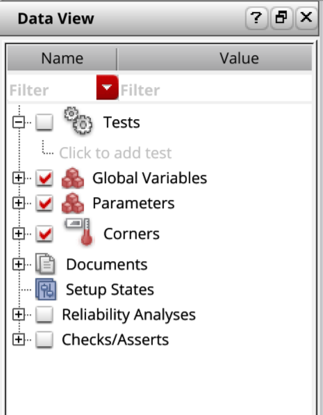
ADE Explorer will open, where you will configure the test. The auto-generated test names (e.g., yourUNI_inverter_test_1) are long and provide zero insight into the purpose of each test, so it is good practice to rename them according to their intentions.
inv_tran_response by clicking the test name once (which will highlight the test in gray), waiting briefly, and then clicking it again to edit the name. Do not double-click. Also, make sure your cursor is aligned vertically with the Name column before clicking. Clicking in the Value column will return you to ADE Assembler.
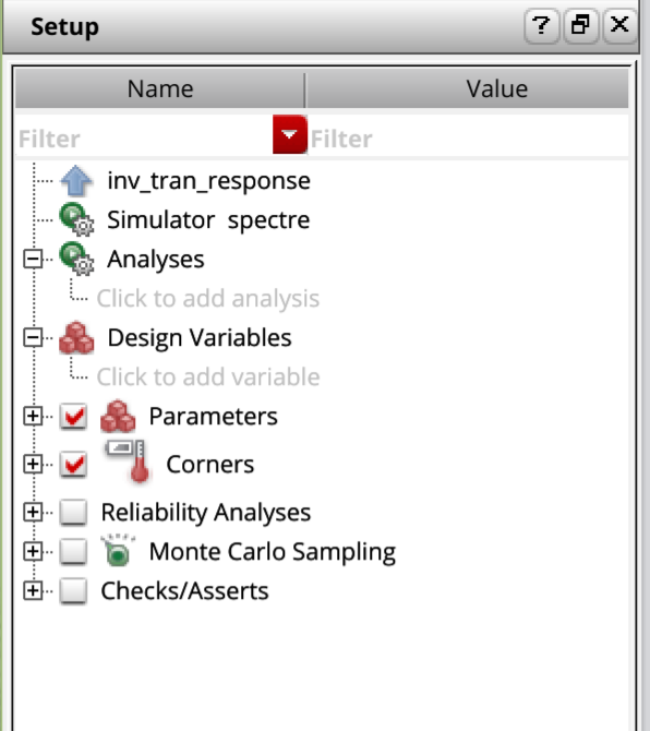
Choose Spectre and a results directory
In Explorer, check that the setup tree shows Simulator spectre. If another simulator is selected, choose Setup → Simulator and select spectre.
Simulation results can occupy substantial disk space, so you don't want this in your home directory which is uploaded to the server. You can use a directory called /workdir instead. In a remote terminal, replace yourUNI with your UNI and run:
mkdir -p /workdir/yourUNI
In Explorer, choose Setup → Save Options. Under Results Location, set Simulation Results Directory Location to /workdir/yourUNI, using your actual UNI.
Raw simulation results in /workdir belong to the current workstation and will not follow you to another workstation. If you get space limit errors while simulating, try emptying the simulation files located in your machine's /workdir directory.
Check the transistor models and temperature
Choose Setup → Model Libraries. The course configuration should automatically supply the TSMC65 Spectre model entries under /courses/ee4321/tech/tsmc65/. These model files are created by TSMC and tell Spectre how the devices (such as pch and nch) behave. Attaching a technology library when creating a schematic does not, by itself, verify the simulation model setup.

Update the 'Section' column entry corresponding to the blue boxed row in the image above from tt to ff to simulate the fast-fast (FF) process corner instead of the typical-typical (TT) process corner, as shown below:

ff to simulate the fast-fast process corner.Choose Setup → Temperature and enter 27 for 27 °C.
Give every design variable a value
In ADE Explorer, choose Variables → Copy From Cellview in the top toolbar. If you have defined any design variables (i.e., by giving names to component parameters instead of actual numbers), they will all be directly copied to the Design Variables section in the Setup panel.
Double-click the Value field next to vdd to numerically define these design variables, and enter 1.0. The supply source and the pulse's high level will both use 1.0 V.
Save your simulation setup
Click the Save icon in ADE to save the setup in the maestro view. Save again after adding analyses, outputs, etc. To resume work in a later session, open inverter_test / maestro from the Library Manager, or choose Open Existing View when launching ADE from the Schematic Editor.
3. Run a transient analysis to observe inverter switching
For a CMOS inverter, when the input goes high, the NMOS discharges the output capacitor and the output goes low. When the input goes low, the PMOS charges the capacitor and the output rises to VDD. A transient analysis lets you simulate this sequence in the time domain.
- In Explorer's Analyses area, click Click to add analysis. You can also choose Analyses → Choose.
- Select tran, enter
5ufor Stop Time, and select moderate accuracy.
Configure the transient analysis with a 5 µs stop time and moderate accuracy. - Check Enabled and click OK. Five microseconds should cover five periods of the 1 MHz input pulse.
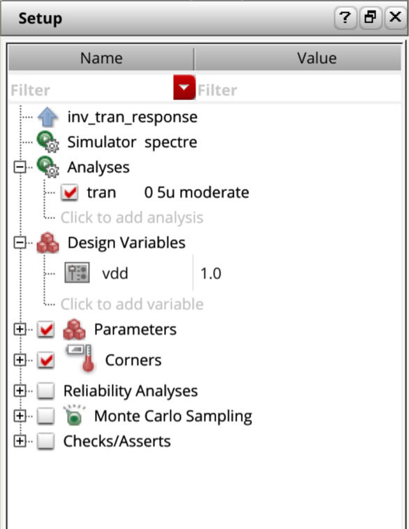
vdd set to 1.0 V.Run Check and Save on any schematic you changed, including the inverter if you edited its devices. In Explorer, click the green Run Simulation arrow in the upper-right section of your screen. ADE will start your simulation.
It is important to understand what ADE does when you click Run Simulation. First, ADE creates an initial netlist containing the top-level instances and the include files. It then generates the complete simulation netlist by bringing in all the transistor-level details of the instantiated cells. In a way, ADE is just a pretty GUI that generates a text-based simulation input (that contains the circuit description, model definitions, simulation settings, and analysis commands) required by circuit simulators. Ultimately, Spectre runs the simulation using the netlist (i.e., a text file) generated by ADE.
You can also go through these steps manually. First, choose Simulation → Netlist → Create to generate and review the netlist, then click Run to start the simulation. This lets you inspect the intermediate netlist output before Spectre is launched.
If you simply click Run Simulation, ADE performs the required netlisting and simulation steps automatically without stopping to show you the intermediate netlist output.
If the run fails, open the simulator log from ADE and read the error message. Usual culprits include undefined variables, missing model files, unconnected terminals, etc. Fix the reported problem and run again.
Plot transient voltages with the calculator
After a successful run, choose Tools → Calculator in ADE Explorer. The ViVA calculator is a very powerful GUI that lets you select waveforms, plot them, and build expressions for measurements.
- Click vt to select a transient voltage. In the schematic window, the status bar will prompt you to select nets or terminals for a VT expression.
- Click the
voutnet. The calculator's expression buffer (the off-yellow box) will showVT("/vout"), as in the image below. - Click Plot, the calculator-and-curve icon circled in red, to display the output voltage versus time in ViVA alongside your schematic. Follow the instructions in the pop-up to undock the graph window and view waveforms in a separate window.
- To add the input waveform to the same plot, keep Append selected in the calculator, click vt again, select
vinin the schematic, and click Plot.

To save an expression in ADE Explorer's Outputs section, click Send Expression to ADE, the gear-and-arrow icon circled in yellow. Add both voltage expressions so you can plot them again by choosing Results → Plot Outputs in ADE Explorer.
Click the Save icon in ADE to save the setup now.
You can also store the expression in the calculator's stack by clicking the green arrow circled in purple. Use Pop & Insert to bring an expression from the stack back into the buffer for building expressions with functions, etc.
For a quick plot directly from the schematic, choose Results → Direct Plot → Transient Signal in ADE Explorer. Click the vin and vout nets, then press Esc to finish selecting signals and display the waveforms.

Now you should see a graph of both the input and output waveforms. Use the trace names and corresponding colors to identify vin and vout.

Measure delay between the 50% crossings
Propagation delay measures the time from an input transition to the corresponding output transition. At a 1.0 V supply, we can use VDD/2 = 0.5 V as the reference level for both signals.
- Zoom into an input edge and its corresponding output edge after the first cycle. Press and hold the right mouse button, then drag to draw a rectangle around the area you want to zoom into. Release the button to zoom into the selected area. You can always return to the full waveform view by pressing f or clicking the Zoom to Fit button. Click the Combine All Analog Traces button on the ViVA window if the signals appear in separate strips.
- Press h in the waveform window to create a horizontal cursor and place it at 0.5 V.
- Use the waveform legend to identify
vinandvout. Press a near thevinwaveform's crossing of the 0.5 V horizontal cursor to place marker A on the input. Press b near the correspondingvoutcrossing to place marker B on the output. You can move markers by dragging them along the waveform. - For a rising input and falling output, record
dx(i.e., time delay) astPHL. You can delete the markers by choosing Marker → Delete All or pressing Ctrl+E. - Repeat for a falling input and rising output. Record this delay as
tPLH.
The average propagation delay is given by tp = (tPHL + tPLH) / 2.

tPLH. Measure your own crossings!4. Run a DC sweep to find the inverter's switching region
In the example above, we used transient analysis to examine the delay of an inverter in response to a nearly step-like input in the time domain. However, transient analysis is only one of the many powerful analyses provided by Spectre.
In this section, you will perform another important simulation called DC analysis. DC analysis is especially useful for analog circuits with consistent bias current (class-A category) because it allows you to determine the circuit's operating point. Remember that everything about your circuit is garbage if the operating point is not correct.
In particular, you will perform a DC sweep. A DC sweep calculates the settled output at each input voltage. The resulting voltage transfer characteristic, or VTC, shows where the inverter changes from a high output to a low output.
If the inverter_test schematic is not already open, go to the Library Manager and open inverter_test again.
Keep the pulse source in the test circuit so that you can return to the transient experiment. Select the pulse source, press q, and set its DC voltage field to vin_dc. Keep other fields unchanged. Run Check and Save.
Return to ADE Assembler. In the Data View panel, expand Tests and click Click to add test. Check that yourUNI library, the inverter_test cell, and the schematic view are selected, then click OK.
In the ADE Explorer window that opens, rename the new test to inv_dc_sweep using the same method described earlier. Configure this test with the same Spectre simulator, model libraries, temperature, and results directory used for the transient test.
In Explorer for inv_dc_sweep, choose Variables → Copy From Cellview and give vin_dc the value 0. Set vdd to 1.0. The DC analysis will sweep vin_dc.
- Click Click to add analysis and select dc.
- Check Save DC Operating Point. Under Sweep Variable, select Design Variable and choose
vin_dc. - Set the sweep range to Start-Stop, with start
0and stop1.0. Choose a Linear sweep with a step size of0.01.
Set the DC sweep range and step size as shown. - Check Enabled and click OK.
- Click the green Run arrow. Wait until the simulation finishes.
Plot the voltage transfer characteristic
You can configure ADE Explorer to plot selected outputs automatically after each simulation. Choose Outputs → To Be Plotted → Select on Design. The schematic editor window will open. Click the vin and vout nets to select their voltages for plotting and press Esc. The selected signals will appear in the Outputs area. Make sure plotting is enabled for both outputs. You can also use the calculator as before, but use vdc instead of vt.

vin and vout signals are added to ADE Explorer's Outputs area for plotting the DC sweep.Save the ADE setup and click the Plot Outputs button (located two buttons below the green Run arrow and directly below the Stop Simulation button) to plot the selected outputs. The vout trace gives the inverter's VTC as shown below. The horizontal axis is the swept variable vin_dc in volts. The vertical axis is the voltage of each selected signal, also in volts. The vin trace follows the swept variable and appears as a diagonal line (y=x), while vout falls as the inverter switches.

5. Compare transistor strengths with a parametric simulation
Parametric analysis repeats the analysis configured in ADE while varying an additional parameter, simulating how a plot of y versus x changes with a third variable z. Before running parametric analysis, add the signals or expressions you want to compare to the Outputs section (like we just did) and enable plotting so you can visualize the results for each parameter value.
Here, you will repeat the DC sweep while varying the NMOS multiplier (the number of parallel devices) and holding the PMOS multiplier fixed. This will effectively change the strength of the NMOS relative to the PMOS. As a result, each NMOS multiplier value will produce a different VTC.
- Open
inverter / schematic. Set the NMOS Multiplier field tonmos_multiand the PMOS Multiplier field topmos_multi. Leave Number of Fingers and the width and length fields unchanged.
Use pmos_multiandnmos_multias the transistor multipliers, which you can control from ADE. - Run Check and Save.
- Return to ADE Assembler and open the existing
inv_dc_sweeptest from the Tests section in ADE Explorer. In Explorer, choose Variables → Copy From Cellview. - Set
pmos_multito10. - Double-click the Value field next to
nmos_multi. Click the three dots (...) to configure its sweep. Click the Add Specification drop-down menu. Select From/To, set From to1and To to20. Choose Linear for Step Type and enter a step size of1. Click OK.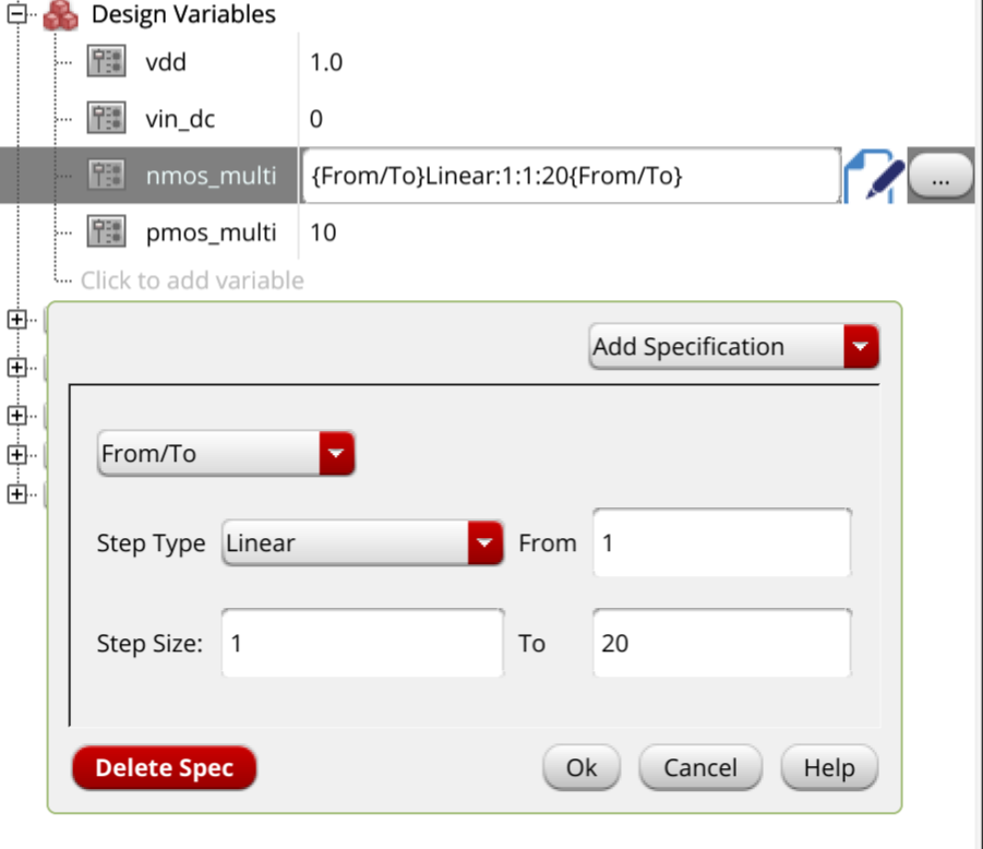
Configure nmos_multito sweep from 1 to 20 in linear steps of 1. - Make sure you have kept
vddat1.0and enabled the dc analysis that sweepsvin_dcfrom 0 to 1.0 V. - Save the ADE setup and run the simulation.

You should get a plot that looks like this.
Increasing the NMOS multiplier strengthens the pulldown path relative to the fixed PMOS, so the switching region should move toward a lower input voltage (which is what we see in the plot above).
You can now run simulations in ADE
You can now place your circuit in a testbench, configure analyses in ADE, run simulations with Spectre, and view and interpret the results in ViVA.
Continue to draw the inverter layout in the Layout Editor.