

If you haven't read the General information page
or the Getting started... page, READ THOSE FIRST.
In this handout, we are going to learn how to draw schematics in Cadence Schematic Editor. We will draw a simple inverter in Composer and then do a transient simulation using the Analog Design Environment. Follow the steps :
Step 1: Invoke cadence by typing
virtuoso &
from your ~/Cadence directory.
Step 2:Click on
Tools--->Library Manager....The library
manager window should pop up soon.
Step 3: Click on
File ---> New ---> Library
.
Step 4: On the "New Library" window, name your library "yourUNI".
Step 5: A "technology file for new Library" window pops up. Click on
attach to an existing technology library and click
cms9flp
.
Step 6: Your library should now be listed in the library manager's "Library" section.
Step 7: In the library manager window, Click on the library you just
created and choose
File ---> New ---> Cellview
.
Step 8: On the "new file" window, which popped up, enter new cell name next to the tab Cell (name it 'inverter' this time) . Make sure that the library name should be same as what you gave , view name should say "schematic" and type should say "composer-schematic". If the "type" shows something else, you can click on the button and choose "schematic".
Step 9: Hit 'OK" and a schematic editing window pops up showing the library name (yourUNI), cell name (inverter) and view name which is "schematic" in this case.

Step 10: Now you are ready to draw a schematic in this window which will finally look as shown in the figure below. Look around for a few seconds and make yourself comfortable with the GUI.
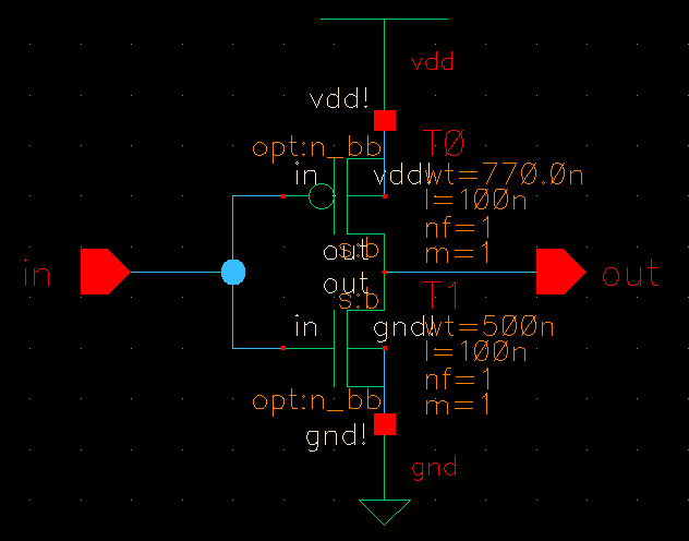
FIG 1
Step 11:
First we will place the nmos and pmos for the CMOS inverter. Choose
from the top bar,
Create --> Instance
. Click Browse next to library name to open the Library browser - add instance window. Choose
cms9flp
for the "library" ,
pfet for the "cell" and
symbol
for the "view".
Now you will see a new window called "add instance" with all of the details of
the pmos you will be placing down soon.

Notice that there are
four terminals on the pmos including the bulk/base, and the length is
100nm.. This is
close to the smallest possible channel length (90nm) for the
IBM technology which we are using. Fill
770n
in the "width single
finger" and move your mouse over the schematic window. A pmos transistor symbol will follow your mouse pointer. Place the pmos device on the window and hit "Esc". Note : In cadence, whenever, you are in the middle of a command, hit "Esc" to end it.
Try hitting it multiple times to make sure you are done with a command.
* You can navigate the schematic with your
middle mouse button.
Scrolling - vertical movement
Scrolling while pressing shift key - horizontal movement
Scrolling while pressing ctrl key - zoom in and out
Step 12: Again choose
Add --> instance
(or you can press 'i') and click 'Browse'. This time find the
nmos in the "cell" and
500n
as the "width all fingers". Again note that there are there
are four nodes in the symbol including the base. Move your mouse over the schematic window and place the nmos transistor vertically below the pmos as in FIG 1 above.
* If you want to go change properties of any
instance on your schematic,
press the symbol and press 'q' as a shortcut.
Step 13: Now we will make wiring connections. choose
Create --> wire (narrow)
and click on the drain of pmos. A wire segment will follow your mouse. Bring the mouse pointer over the drain of nmos and click it to complete the wire section. Hit "Esc" on your keyboard to end the command. Similarly, draw all the wires shown in blue in
Fig 1. above.
* The shortcut for adding wires is 'w' on your schematic screen.
Step 14: Put the pins "in" and "out" by choosing
Create -->pin
and giving "in" and "out" for "Pin names" one by one. Make sure to choose "direction" as
input
for "in" and
output for "out". Other options on the "add pin" form remain unchanged. Place the pins as shown in FIG 1.
* Name ALL pins and nets are in
lowercase
letters and numbers (no special characters like # ! @ *) throughout this course!
Step 15: To make this schematic a
functioning inverter we need to define DC voltages at the inverter's Vdd and
ground nodes. This can be done using supply nets from the analogLib library, which map to
global power rails. Place the 'vdd' and 'gnd' components at the appropriate nodes.
Step 16: Congratulations! You have just completed your
first schematic in Cadence. To check and save your design, click on the icon with a box and a check mark. You will be warned if you have any floating wires or pins. You can also perform the same function by selecting
Step 17:
Now we will make a symbol for this schematic, just like the pmos/gnd symbols.
From your Schematic Editor window, choose
"Check and Save" from the
File menu of the schematic window.
Create --> Cellview --> from Cellview...
A new
Cellview from cellview window pops up. Everything should be already set on this window by default.
The library and cell names should match those of your current schematic. It should look like figure 2. Click OK, and a "Symbol
Generation Options " window will pop up. This is where you decide where you will
have your pins located on the symbol. The defaults are generally sufficient for blocks with just a few inputs; just click OK here as well. You will then be presented with your symbol in a symbol editor window.
This doesn't REALLY look like an inverter symbol, but it doesn't matter for simulation. If you are really keen, you can modify this symbol using the graphic tools available on this window so that it really looks like an inverter symbol, but that's not mandatory.

FIG 2.

FIG 3.
Step 18: Close both windows (schematic and symbol) and click here to move on to the simulation part .
Here is a summary of some useful shortcut
keys:
c --- copy instance
w --- draw wire
m --- move instance
q --- instance properties
i --- add instance
f --- zoom to fit (show all components in schematic)
del --- remove
scroll + shift --- horizontal movement
scroll + ctrl --- zoom in-out
right-click mouse drag --- zoom to area
esc --- quit function
Make sure to hit esc after each function, since some functions will continue to affect your schematic when you don't want them to. Note that you will have to select an object after you hit a function key; for example, to copy an instance, press 'c' first -> click what you want to copy -> then click again at the desired location.