CMOS fluorescence-based active microarrays
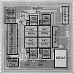
This project is a multidisciplinary effort to novelly exploit CMOS silicon microelectronics in the design of  low-cost, portable, self-contained “gene chip” technology for nucleic acid measurement and detection. Much of this effort is focussed on developing active substrates based on fluorescence detection. One such active microarray is shown below, capable of time-resolved fluorescence detection for background rejection (though time-gating) and fluorescence-lifetime measurement. DNA probe is attached directly to the chip surface for detection.
Related Publications
T.-C. Huang, S. Sorgenfrei, K. L. Shepard, P. Gong, and R. Levicky, “A CMOS array sensor for sub-800-ps time-resolved fluorescence detection” IEEE Custom Integrated Circuits Conference, 2007.
Abstract
This paper describes the design of an active CMOS sensor array for fluorescence applications which enables timegated, time-resolved fluorescence spectroscopy. The 64 x 64 array is sensitive to photon densities as low as 8 x 10⁶ photons/ cm2 with 64-point averaging and, through a differential pixel design, has a measured impulse response of better than 800 ps. Applications include both active microarrays and high-frame-rate imagers for fluorescence lifetime imaging microscopy.
D. E. Schwartz, E. Charbon, and K. L. Shepard, “A single-photon avalanche diode imager for fluorescence lifetime applications” Symposium on VLSI Circuits, 2007, pp. 144-245.
Abstract
A 64-by-64-pixel CMOS single-photon avalanche diode (SPAD) imager for time-resolved fluorescence detection features actively quenched and reset pixels, allowing gated detection to eliminate pile-up nonlinearities common to most time-correlated single-photon counting (TCSPC) approaches. Reset Timing information is collected using an on-chip time-tocalb calibrated digital converter (TDC) based on a counter and a supply- interpolators regulated delay-locked loop (DLL).
G. Patounakis, K. L. Shepard, and R. Levicky, “Active CMOS array sensor for time-resolved fluorescence detection” IEEE Journal of Solid-State Circuits, November, 2006
Abstract
Surface-based sensing assays based on fluorescence-based detection have become commonplace for both environmental and biomedical diagnostics. Traditional array scanners are expensive, large, and complex instruments. This paper describes the design of an active CMOS biosensor substrate for fluorescence-based assays that enables time-gated, time-resolved fluorescence spectroscopy without the need for an external reader. The array is sensitive to photon densities as low as 1 15 108 cm2, has a dynamic range of over 74 dB, and has subnanosecond timing resolution. Sensitivity is achieved through subsampling and averaging.
G. Patounakis, K. L. Shepard, and R. Levicky, “Active CMOS biochip for time-resolved fluorescence detection” Symposium on VLSI Circuits, 2005.
Continue reading →
 Our most recent array design was capable of a maximum frame rate of 3.9 Hz and consisted of a 64 x 64 SPAD array with integrated timing and pixel control circuitry in 0.35μm technology. The image on this page below shows a FLIM image of quantum dots (in color) next to a CCD image showing the location of the quantum dots on the array.

 A thin-film bulk acoustic resonator (FBAR) can be employed as the micron-scale equivalent of a quartz crystal microbalance (QCM); mass attaches to the surface of a piezoelectric crystal, causing the resonance frequency to decrease slightly. Whereas a quartz crystal sensor operates in the megahertz regime, FBAR structures resonate in the low gigahertz regime. Their small size allows array integration of sensors, similar to a microarray, and the increased frequency allows increased sensitivity. Both of these features make FBARs ideal for direct CMOS integration, where sensors can be built in dense arrays and used without bulky external measurement equipment.
 In this research, we have fabricated FBAR structures monolithically on a custom CMOS substrate. The resonators are solidly mounted, and mechanical isolation is achieved with a multi-layer acoustic reflector. Monolithic fabrication enables an array of integrated resonators, and the underlying CMOS circuitry forms an independent FBAR-CMOS oscillator around each device. The CMOS substrate also contains a dedicated digital frequency counter for each oscillator, enabling parallel on-chip
 On-chiposcillators at 850 MHz and 1.45 GHz have been demonstrated, and the integrated sensors have a mass sensitivity many times higher than that of a traditional QCM. In addition to sensing, this methodology may find significant utility in RF applications, where it enables monolithic integration of high-Q elements directly on a standard CMOS substrate.