

In this handout, we are going to learn the following :
By now, you would have known how to enter and simulate your designs using Spectre. The next step in the process of making an integrated circuit chip is to create a layout. What is a layout? A layout is basically a drawing of the masks from which your design will be fabricated. Therefore, layout is just as critical as specifying the parameters of your devices because it determines whether yours is a working design or a flop!
There are 2 ways of doing a layout: manual and automated. Manual layout usually enables the designer to pack his devices in a smaller area compared to the automated process but it is more tedious. The automated process, on the other hand, is done using standard cells and usually takes more real estate space but it is much faster. In this tutorial, you will learn how to perform manual layouts and a simple inverter layout will be shown.
Before we get into the layout, first you need to understand the design rules for layout. The design rules which we will be using is the TSMC 65nm CMOS Rules. Design rules give guidelines for generating layouts. They dictate spacings between wells, sizes of contacts, minimum spacing beween a poly and a metal and many other similar rules. Design rules are essential to any successful layout design, since they account for the various allowances that need to be given during actual fabrication and to account for the sizes and the steps involved in generating masks for the final layout. The design rules that we will be using can be found on the VLSI lab computers at /courses/ee4321/tech/tsmc65/T-N65-CM-SP-018-K3_MOM/Base_PDK/T-N65-CL-DR-001/TN65CLDR001_2_1.pdf . You can read pdf's directly in the command window by typing (evince filename.pdf). Note that the layout is very much process dependent , since every process has a certain fixed number of available masks for layout and fabrication. For the case of this tutorial, we are using a TSMC 65nm CMOS process, which supports one poly and 10 metal layers.
1. Here we will create a
layout for the inverter cell.
In the CIW window, click on the File
--> New --> CellView. Choose Library as 'yourUNI', CellName as 'inverter' and View
Name as 'layout'. Make sure that type is 'Layout' and Open with is 'Layout XL' . Then click on the OK button.
The Layout editor window will show an empty space to lay out your cell, as well as a column on the left of the window deataling all the layers like nwell, pwell, metal, and oxide diffusion (active) layers etc.
for the given process. An alternate way to open the layout editor
window is to click on ""Launch-->Layout XL" A Startup Option Dialog Box will pop up; check the 'Create New' option of Layout section, and keep the Configuration section checked as 'Automatic', as shown below.
The LSW window should look something like this:

In Layout editor, components do not move freely, instead moving along certain angles and snap to the grid. Therefore, for better cursor movement, it is crucial to follow these steps:
1. Go to
Options -->
Display
and ensure your display options settings look as follows. You can
save these settings by doing 'Save to' and pressing OK.

2. Go to
Options --> Editor
and at the top middle box,
make sure 'gravity on' checkbox is not ticked.
We are ready to draw objects in the layout window. Go to Create-> Instance . Take the nfet device from Library Browser as it is shown below. Do not forget to pick layout view. After you place the transistors on the layout window, you can change the sizes by clicking on your transistor with your mouse and then you can press Q on your keyboard.

Then, we need to create the necessary pins as well. Go to Create -> Pin. Name the terminal name appropriately, selecting the mode as 'manual'. Then pick the I/O type as input. Put a checkmark on Create Label and select auto. After that, click on options. You can write height as 0.2 . Then, click OK. Then, Select M1 pin from the LSW window. Then, draw a rectangle with mouse's left click. Do not size the rectangle too big or small. (You can see a proper size for a pin on the following screenshots.) Place the pin somewhere available on the layout window. Click on the 'text' on the pin that you created, make sure the layer is M1 layer.
There is an easier way to generate all components from your schematic. Go to 'Connectivity-->Generate-->All From Source'. Make sure your dialog box looks as follows:


After instantiating all components from schematic cellview, your layout editor screen should look like the following below:
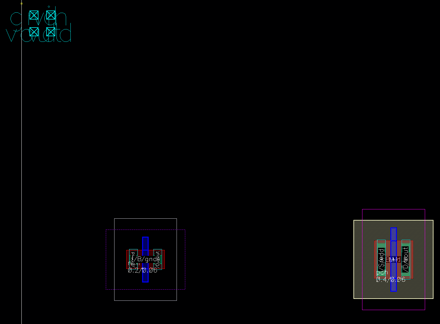
Now that you have placed all
components, you need to make connections between
them to create an inverter. We also need to place substrate and n-well contacts. Before drawing any wires, you
need to select the correct drawing layer from the layer selection window (LSW) . First choose "M1
drw" from LSW . Now try drawing some wires with
create --> shape --> rectangle
(shortcut 'r')
or
 create --> shape -->
path (shortcut 'p').
Note that drawing paths is a little tricky. You will need to practice a little bit.
To end a path you have to double click with your left mouse button.
Generally drawing rectangles are easier to draw and edit. If you have drawn a rectangle of any layer and need to edit its location or dimensions, press 's', then drag your cursor into a box enclosing the specific part that you want to edit. For instance, you can enclose a corner, or you can enclose an edge of the rectangle and edit accordingly.
Now add in the wire connecting
the drains of both nmos and pmos which will serve as the output of the inverter. Do the same
for the poly connection between the gates. You can do this by choosing "pc drw" from LSW. Note that
create --> shape --> path automatically chooses min. width for the path. To change this, you need to
hit F3 while the command is active and an option form will appear in which you can change the width.
By using 'rectangle'
or 'path'
, you can also make
vdd and gnd buses
(vdd on top of pmos and gnd on bottom of nmos) with metal layer M1. Also connect the source of pmos to this
vdd bus and
that of nmos to gnd bus using the 'M1 drw' layer. Note that everything is manual
when drawing layouts; connecting the substrate of the pmos to Vdd should be done
by hand as well. Extend the n-well of the pmos to reach into the vdd bus on the
top. You can do this by using the 'NW drw' layer.
One useful tool is the ruler. You can draw a ruler by hitting 'k'. With it you can align the vdd and gnd buses, and keep there sizes symmetrical. To remove all rulers on the screen, press shift + k.
* If you are in the middle of any command such as 'm', 'p' or 's', hit F3 and an option form will appear specifically for that command. You can generally solve most of the problems by choosing various options from this form which can be applied to the currently active command.
Then move your pins to the correct location. Have each pin in contact with an M1 layer of the same net. So your VDD pin, for instance, can be anywhere on top of your VDD bus. One important fact here is to make sure that the label moves with the pin. Each label (the pin name in text) will have an '+' mark in its center. If this '+' mark is not on top of the same net that the pin is, you will get an error in LVS regarding port mismatch.
Now we should add vias (also called
contacts), which are vertical connections between two different layers. For
example, an M1_M2 via would enable conduction between the two metal layers M1
and M2. To place the substrate and n-well vias, choose
create --> via (shortcut 'o')
. From the tab that says 'via
Definition', you can choose the via that you want to use. Check the 'Use All Vias' checkbox. In our inverter
layout, we can use three vias:
1) connecting the 'vin' pin made of the M1
layer with the two gates made of the PO layer
2) connecting the
n-well of the PMOS with the VDD bus M1 layer
3) connecting the NMOS p-substrate
with the GND bus at the bottom
Note that we can get rid of the bulk connections vias in (2) and (3) by enabling bodytie_type parameters of the nmos and pmos instances, as will be shown later. That way, only the M1-PO via needs to be placed. For now, we will use vias though.

To add Via 1, go to Create --> Via, and select M1_PO. A via essentially consists of 3 or more layers, but the main thing to consider is the contact layer and the two layers being connected, in this case an M1 layer and PO layer. Hence, place the via such that it tocuhes both the PO layer between the two gates AND the M1 layer. As you see below, there must be some area of the PO layer connecting to the via overlapping with the PO layer of via; similarly, there must be some area of the M1 layer connecting to the via overlapping with the M1 layer of via. An easy way to do this is to have the PO and M1 layers overlapping in the first place, and then placing the via where they overlap. As a useful note, it is unnecessary to have both layers overlap with the contact, as during fabrication any overlapping layers of the same type are considered the exact same layer shape.

Before we draw Vias 2 and 3, there are 3 layers to study: The OD layer (red slashes) and the NP and PP layers. The layer 'OD' stands for 'Oxide Diffusion' and it defines both p- and n-type active areas. It is where the doping takes place, to form Source, Drain, and Bulk areas for instance. If the active layer is over an PP-layer (p+ implantation/diffusion layer), it represents a p-type diffusion area; if the active layer is on top of a NP layer (n+ implantation/diffusion layer), it represents an n-type diffusion area. NP and PP layers are outlined boxes with no fill, so it may be difficult to view; in order to view, you can turn off the layers under 'Visibility' column of the LSW window.

Source: http://en.wikipedia.org/wiki/File:Cmos_impurity_profile.PNG
The drawing above shows us a sideview of
a PMOS and NMOS put together. For the NMOS, the substrate will be of p-type
and it should be connected to GND. So we will do this with a via consisting of an OD + PP layer
connected to the GND metal layer. (Via 3)
For the PMOS, the substrate will be of n-type and it should be connected to
Vdd. So we will do this with a via consisting of OD + NP layer. Make sure the n-well of this via is contiguous with the n-well of the PMOS. (Via 2)
Let's place Via 2 first. Instantiate a M1_NW via, making sure the NW layer of this via overlaps with the NW layer of the PMOS. Then connect the M1 layer between vdd pin and the M1 layer of the via. Make sure the NP and PP layers DO NOT OVERLAP (overlapping NP and PP layers causes DRC errors). This ties the n-well of the PMOS to VDD, just like in the schematic.
Similarly, this time we can connect the bulk of the NMOS with GND (Via 3). This time we need the bulk to be of the p-type, so we need the via to consist of both the OD + NP layers. First place a M1_SUB via to overlap with the GND bus.
It's important to note that DRC may throw errors for unsufficient OD and NP/PP layer areas in the vias. You can simply resolve this by drawing corresponding layers in bigger rectangles on top of the vias. After all this exercise, your layout should look like as below :

Connecting bulks of NMOS and PMOS transistors using vias can get cumbersome. Another way is to simply enable bodytie_type parameters. Press 'q' on an nmos or pmos instance you'd like to enable this for; go the 'Parameter' tab, scroll down to 'bodytie_typeR' or 'bodytie_typeL' parameters. Change either (NOT BOTH) parameter to 'Detached'. Now you can simply connect M1 layers to the bulk contacts, without having to worry about DRC violations regarding OD and NP/PP layer area constraint. Layout now looks like this with this parameter enabled:

Note that you can view only desired layers by clicking the 'NV' button in your LSW window. Select desired layers by left-clicking, and deselect unwanted layers by right-clicking your mouse. Then go back to your layout screen and repeat Ctrl + f and Shift + f. This is extremely useful when trying to figure out what a cell is composed of, and also locating faulty connections. You can also go back to viewing all layers by clicking on the '+' button under 'Vis" column.
Note also that you can add new pins by hitting hitting ctrl + p. If you have deleted a pin by mistake, or want to make new pins, press ctrl + p and define desired properties. Especially watch out for the metal layer, metal type, label size and type (If your pin is of M1 pin material, label your pins with M1 pin).
Summary of
shortcut keys, in addition to those mentioned in the
Tutorial on Schematic Editor :
r --- draw rectangle
p --- draw path (very finnicky, so not recommended)
k --- ruler
s + drag cursor onto an edge or corner --- edit edges or corners of a rectangle
m --- move object
shift + f / ctrl + f --- display or not display layout metal contents
F3 in the middle of a function --- options to that function